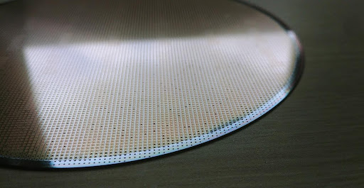
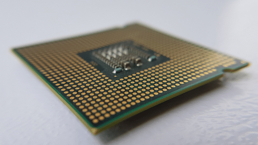
Microchip production is a complex series of material deposition and removal steps performed on silicon wafers. Toward the end of this process, metal bumps are formed to enable electrical connections between the chip, its final package, and external components.
One of the last steps traditionally included a plasma etch process, used to remove a thin film of refractory metal between the bumps. This step was assumed necessary to ensure electrical isolation—until deeper analysis suggested otherwise.
A recurring issue plagued the production line: the longer the delay between the plasma etch process and final wafer testing, the more defective dies were found. This time-dependent yield degradation posed a major risk to quality and efficiency.
The typical solution focused on logistics. Operations teams worked to minimize the “dwelling time”—the interval between plasma etching and wafer testing—to reduce yield loss. While this provided short-term relief, it did not address the root cause. Instead, it introduced more scheduling pressure and operational complexity.
Using the PRIZ innovation platform, engineers applied Root Cause Analysis and Functional Modeling. The analysis revealed that the plasma etch process was contaminating the bumps, compromising their integrity over time and directly causing the observed yield degradation.
Rather than attempt to fix or optimize the plasma etch step, the team took a bold and counterintuitive path: eliminate the operation altogether. Through careful process redesign, its function was transferred to an earlier step in the flow that did not affect bump quality.
This strategic process step elimination not only resolved the quality issue but also simplified the overall manufacturing sequence.
The outcome was immediate and significant:
“We didn’t just improve the process. We removed what didn’t belong—and the problem disappeared with it.”