creative tool
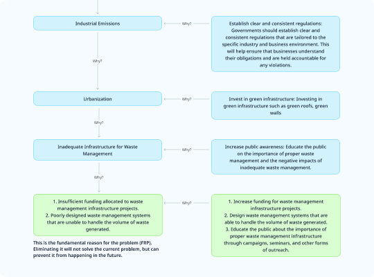
The 5 Whys tool is a commonly used method for Root Cause Analysis. It is often seen as a simple process of asking the question ‘Why?’ five times to uncover the underlying reason behind a problem. However, this perception is not entirely accurate. The 5 Whys is actually a powerful creative thinking tool designed for thorough problem analysis and resolution.
Here, we present a modified version of the 5 Whys tool, incorporating concepts developed by PRIZ Guru Inc. This modified version offers the following key features:
The 5+Whys technique is a valuable tool for creative thinking that helps break free from psychological inertia. It redirects our focus towards a logical analysis of sequential causes and effects. By utilizing this tool, we can achieve a deeper understanding of systems and generate effective solutions. Here are some notable benefits associated with using the 5+Whys technique:
The 5+Whys tool is highly effective in providing quick responses and is invaluable in various scenarios. It is especially useful for addressing unexpected parameter deviations (excursions) and analyzing and resolving chronic problems. Some notable applications include:
Furthermore, the 5+Whys thinking tool is versatile and can be applied in numerous other contexts to harness its creative problem-solving potential.
The process is related to microelectronics - microchip manufacturing. The purpose of the process is to create a SiO2 layer on the surface of a Si wafer. Equipment: Vertical furnace to heat the wafers in the Q2 atmosphere and perform oxidation on the wafer surface. Process: The oxidation occurs on the front side and on the back side of the wafer Requirements: Create a SiO2 thin layer with a certain thickness and low sigma - low standard deviation of the thickness between the wafers and within the wafer Failure: Wafers from the lower zone have higher thickness and significantly higher within wafer sigma (standard deviation of the thickness within the wafer)

Wet cleaning is widely used in microchip manufacturing. Single wafer equipment is working as follows. A wafer rotates, and chemistry is poured from a movable nozzle. Water rinsing is performed at the end of the process. Loading of a new batch of the chemistry resulted in excursion - a strongly increased amount of defects was observed on the wafer after the processing. The project is dedicated to the failure analysis and creation of innovative solutions.
This project investigates radial non-uniformity of CDO low-k dielectric deposited by PECVD and its possible impact on wafer performance. Final test data indicate that faster dies are mainly located closer to the wafer center, while slower dies are more often found near the wafer periphery. The corresponding RC-delay trend also increases toward the wafer edge. The focus of the project is the capacitance component of RC-delay. CDO is expected to provide a low dielectric constant between BEOL metal lines, but the deposited film may not have uniform properties across the wafer. Near the wafer edge, the process can be influenced by different gas flow, plasma behavior, residence time, temperature, and pumping conditions. This may lead to stronger oxidation and deeper precursor decomposition near the periphery, forming CDO that is more oxygen-rich, less carbon-rich, denser, and closer in behavior to SiO₂. As a result, the dielectric constant k may increase toward the wafer edge, causing higher interline capacitance, higher RC-delay, and lower die speed. The project uses Functional Modeling to understand how PECVD chamber components and process conditions affect CDO film properties. The goal is to identify the main functional and problematic interactions and propose directions for compensation, such as radial gas-flow tuning, multi-zone showerhead design, edge compensation flow, and local plasma or temperature control.

This project investigates the nonuniform erosion of an expensive Ta sputtering target during Ta/TaN PVD. A deep racetrack groove forces target replacement while a significant amount of tantalum remains unused. Using PRIZ problem-solving tools, the project explores the system’s functions, identifies the root causes of localized erosion, and develops ways to improve target utilization without reducing deposition rate or production throughput.
This project applies Functional Modeling to analyze the single-wafer wet etch process in semiconductor manufacturing. The model shows that wet etch defects are not caused only by chemistry, but also by interactions between the wafer, liquid flow, air, rotation, rinsing, drying, drain, and chamber environment. Key challenges include incomplete wetting, trapped air or bubbles, residue and particle redeposition, evaporation-driven watermarks, and contamination during rinse or drying. The project identifies improvement directions such as better wafer pre-wetting, controlled airflow, reduced evaporation, optimized rinse and drying conditions, and alternative chamber concepts such as face-down processing in a shallow liquid bath.
This project investigates particle-defect formation during SiO₂ dry etch. Functional modeling revealed that defects can be generated by two coupled mechanisms: chemical formation of SiO₂/SiOFₓ particles from SiF₄ interaction with moisture, and mechanical generation of particles by excessive ion bombardment and sputtering. The proposed improvement direction is to balance chemical etching and ion-assisted etching by properly adjusting the source and bias generators, reducing moisture, improving by-product evacuation, minimizing sputtering, and using pulsed or multi-step process recipes. The goal is to reduce particles and micromasking while maintaining etch rate, profile control, and process stability.
This project investigates how to increase the copper removal rate during Chemical Mechanical Planarization (CMP). Functional modeling revealed that increasing H₂O₂ alone is ineffective beyond an optimum level because rapid oxidation creates a thick, passivating Cu₂O/CuO layer that must be mechanically removed. The winning direction is to balance faster oxidation with stronger mechanical removal by optimizing pad speed, abrasive concentration, pressure, conditioning, and slurry transport.
Semiconductor devices are becoming more complex and expensive. But what exactly are we paying for when we buy a computer, cellphone, or any device containing a microchip? It’s not for radically new functions—the core components remain the same: transistors and interconnections. According to Moore’s law, transistors are getting smaller, with more interconnection layers added, making the manufacturing process longer and more costly. In reality, we’re paying for the inability of engineers to efficiently solve engineering challenges. This project leverages System Functional Modeling (SFM) to analyze the IC interconnection layer and Process Functional Modeling (PFM) to evaluate its manufacturing process. These analyses aim to deepen our understanding of both the device and the production process, generating innovative solutions for cost reduction and improved efficiency.