creative tool
The 40 Inventive Principles is a basic TRIZ tool that assists in problem-solving, generating new ideas, and creating innovative solutions. Genrich Altshuller developed the technique’s fundamentals by analyzing, classifying, and systematizing tens of thousands of patents.
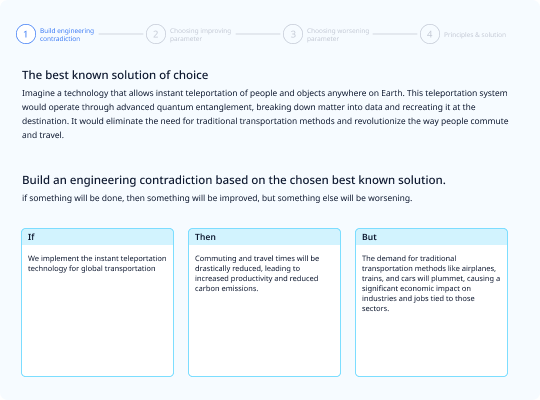
40 Inventive Principles is a creative thinking tool that helps us to free from psychological inertia and makes us think “out-of-the-box”. 40P redirects the problem-solving process from guessing and intuitive decisions to creative analysis and innovative solutions generation. Here, we want to summarize how you and your team can benefit from the 40P tool:
The 40 Inventive Principles thinking tool is useful in various cases of parameter improvement. Some highlighted cases include:
From here, you can further explore and discover many other situations where the 40P thinking can be useful.
Wet cleaning is widely used in microchip manufacturing. Single wafer equipment is working as follows. A wafer rotates, and chemistry is poured from a movable nozzle. Water rinsing is performed at the end of the process. Loading of a new batch of the chemistry resulted in excursion - a strongly increased amount of defects was observed on the wafer after the processing. The project is dedicated to the failure analysis and creation of innovative solutions.
Flash heating of a wafer is widely used in microchip manufacturing. The purpose of the process is to prevent the diffusion of ions and atoms. During the flash process, a wafer breakage occurs. The project's purpose is to learn and understand the mechanism of the wafer breakage and propose the solutions to prevent the wafer breakage
This project showcases how functional modeling can drive innovation by analyzing and simulating various versions of a vacuum cleaner. By studying the functional model, you will experience firsthand how the Functional Modeling creative thinking tool helps identify opportunities for improvement and generate innovative ideas for the next generation of products. Through this example, you’ll learn how to dissect the functionality of a vacuum cleaner, revealing ways to enhance its performance, efficiency, and user experience—ultimately paving the way for future innovations.
The process is related to microelectronics - microchip manufacturing. The purpose of the process is to create a SiO2 layer on the surface of a Si wafer. Equipment: Vertical furnace to heat the wafers in the Q2 atmosphere and perform oxidation on the wafer surface. Process: The oxidation occurs on the front side and on the back side of the wafer Requirements: Create a SiO2 thin layer with a certain thickness and low sigma - low standard deviation of the thickness between the wafers and within the wafer Failure: Wafers from the lower zone have higher thickness and significantly higher within wafer sigma (standard deviation of the thickness within the wafer)
Copper electroplating is essential for forming advanced semiconductor interconnects, yet radial thickness non-uniformity remains a costly challenge. Thicker deposition at the wafer edge and thinner copper at the center force manufacturers to rely on overplating and CMP compensation, increasing material waste and process cost. Using the PRIZ Platform, this project reveals that the true amplification mechanism lies in operating within a kinetically controlled regime, where small voltage variations caused by seed-layer resistance produce large thickness deviations. By shifting the process closer to diffusion-controlled behavior and reducing sensitivity to voltage fluctuations, uniform deposition can be achieved intrinsically — enabling thinner seed layers, reduced overplating, lower CMP burden, and overall cost reduction.
The project addresses instability in the dissolution of tantalum (Ta) anodes in hydrofluoric acid (HF), where hydrogen gas generated during the reaction becomes trapped in the solution, forming foam that disrupts the process and creates safety risks. Using the PRIZ Platform, a Functional Model of the system was developed. The model revealed that the HF solution is both the most functional and the most problematic component, leading to a physical contradiction: HF must interact with Ta anodes to enable dissolution, but must not retain the hydrogen gas produced during the reaction. Applying the PRIZ principle of Separation in Space, two reactor concepts were proposed: a spray interaction reactor, where HF is pumped to spray onto anodes placed above the solution, and a surface wetting reactor, where anodes are positioned at the top of the solution, allowing natural circulation and easy hydrogen release. Both designs eliminate foam formation and provide a stable, controllable, and safer dissolution process.
Semiconductor devices are becoming more complex and expensive. But what exactly are we paying for when we buy a computer, cellphone, or any device containing a microchip? It’s not for radically new functions—the core components remain the same: transistors and interconnections. According to Moore’s law, transistors are getting smaller, with more interconnection layers added, making the manufacturing process longer and more costly. In reality, we’re paying for the inability of engineers to efficiently solve engineering challenges. This project leverages System Functional Modeling (SFM) to analyze the IC interconnection layer and Process Functional Modeling (PFM) to evaluate its manufacturing process. These analyses aim to deepen our understanding of both the device and the production process, generating innovative solutions for cost reduction and improved efficiency.
To reduce high turnover at the plant the managers propose different ideas, but it does not help. All proposed solutions are good, but there are some of them that are blocking the effectiveness of the rest of the solutions. The purpose of the project is to analyze the proposed solutions (perceptions) and define the blocked. The solutions with high blocking rank should be completed first to ensure the effectiveness of the rest of the ideas. The Perception Mapping (PMap) creative thinking tool was used for the blockers definition.