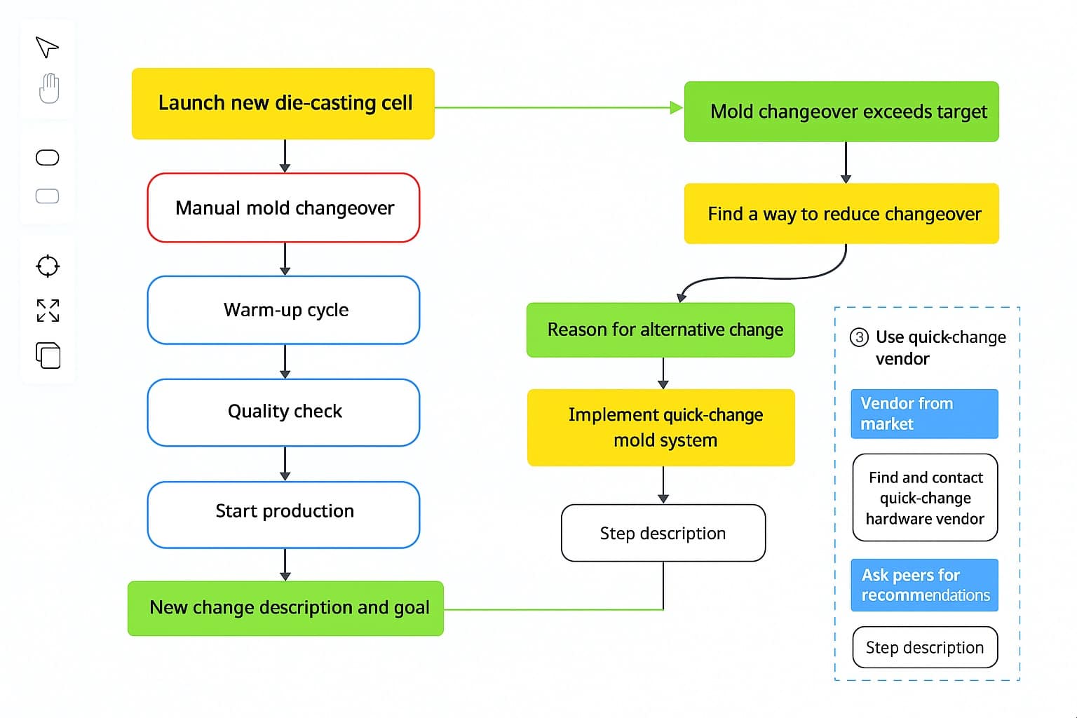
Every improvement project—whether a production line upgrade or an enterprise-wide digital rollout—faces two constant threats: hidden risks and unexpected costs. Change Flow Thinking (CFT) offers a clear, visual way to reveal those threats before they derail your plans. By mapping every decision, resource, and risk on a single tree-flow diagram, teams gain the confidence to push bold ideas forward without gambling on the outcome.
CFT shines whenever the path forward feels murky:
If the cost of getting it wrong is high, Change Flow Thinking helps you get it right—fast.
Ready to experience the framework first-hand? Launch a Change Flow Thinking project in the PRIZ Playground—no credit card, no downloads. Build your first diagram, invite teammates, and follow the guided workflow that turns complex ideas into a low-risk reality.
Innovation stalls when teams drown in spreadsheets and conflicting assumptions. By visualizing the entire change flow, CFT replaces guesswork with clarity. Companies that embed Change Flow Thinking report:
When your people see exactly why each task matters—and how it impacts the big picture—momentum soars.
This project showcases how functional modeling can drive innovation by analyzing and simulating various versions of a vacuum cleaner. By studying the functional model, you will experience firsthand how the Functional Modeling creative thinking tool helps identify opportunities for improvement and generate innovative ideas for the next generation of products.Through this example, you’ll learn how to dissect the functionality of a vacuum cleaner, revealing ways to enhance its performance, efficiency, and user experience—ultimately paving the way for future innovations.
Wet cleaning is widely used in microchip manufacturing. Single wafer equipment is working as follows. A wafer rotates, and chemistry is poured from a movable nozzle. Water rinsing is performed at the end of the process. Loading of a new batch of the chemistry resulted in excursion - a strongly increased amount of defects was observed on the wafer after the processing. The project is dedicated to the failure analysis and creation of innovative solutions.
The process is related to microelectronics - microchip manufacturing.The purpose of the process is to create a SiO2 layer on the surface of a Si wafer. Equipment: Vertical furnace to heat the wafers in the Q2 atmosphere and perform oxidation on the wafer surface. Process: The oxidation occurs on the front side and on the back side of the wafer Requirements: Create a SiO2 thin layer with a certain thickness and low sigma - low standard deviation of the thickness between the wafers and within the waferFailure: Wafers from the lower zone have higher thickness and significantly higher within wafer sigma (standard deviation of the thickness within the wafer)
Semiconductor devices are becoming more complex and expensive. But what exactly are we paying for when we buy a computer, cellphone, or any device containing a microchip? It’s not for radically new functions—the core components remain the same: transistors and interconnections. According to Moore’s law, transistors are getting smaller, with more interconnection layers added, making the manufacturing process longer and more costly.In reality, we’re paying for the inability of engineers to efficiently solve engineering challenges.This project leverages System Functional Modeling (SFM) to analyze the IC interconnection layer and Process Functional Modeling (PFM) to evaluate its manufacturing process. These analyses aim to deepen our understanding of both the device and the production process, generating innovative solutions for cost reduction and improved efficiency.
The integration of CFRP materials into automotive designs presents challenges related to compatibility, performance, and safety, necessitating a careful transition from a Chromolly tubular space frame to a CFRP monocoque. Key considerations include determining the optimal geometry for suspension, aerodynamic features, and the placement of components like the battery pack and sensors, all while adhering to FSAE safety protocols. Additionally, decisions regarding the production method—whether to use preimpregnated carbon fibers or an injection method—must be made early to facilitate timely production. The development process involves creating molds and plugs from suitable materials, ensuring that all assemblies can be connected without compromising structural integrity, and maintaining strict adherence to budget constraints and sourcing of materials.
In response to the potential outbreak of a third world war and the risk of Egypt becoming isolated from global trade and financial systems, this project aims to develop a self-sustaining, decentralized digital ecosystem. The goal is to ensure economic stability, resource accessibility, and secure communication for citizens, businesses, and the government in times of crisis.This solution will be delivered as an application-based platform that integrates barter trade, digital currency, AI-driven supply chain management, emergency communication, and cybersecurity measures. By leveraging blockchain technology, AI-powered logistics, and decentralized networking, the platform will enable uninterrupted trade, resource distribution, and crisis coordination without reliance on external financial institutions or internet-based infrastructure.
To address the requirement for smaller and more powerful processors, innovative 3D packaging is developed, which involves stacking many layers vertically. This enhances performance but produces mechanical difficulties such as wafer bowing as a result of internal tension caused by thermal expansion mismatch. this problem has approached from a materials engineering perspective, investigating how material selection, layer thickness, and deposition conditions may minimize stress and prevent deformation.
The project was dedicated to production yield improvement in microchip manufacturing. The bumps are created on the top of a wafer and used for the final test of all dies. Only good dies are taken for the packaging. All dies that fail the test will be scrapped. The process yield depends on the amount of "good" and "bad" dies. It was revealed that in some cases, the time between the end of the process and the final test impacts the yield. The longer the dwelling, the more dies fail the final test. If the dwelling exceeds hundreds of hours, the amount of failed dies becomes dramatically high, which results in the scrapping of the whole wafer. The problem was analyzed and solved.