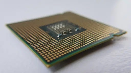
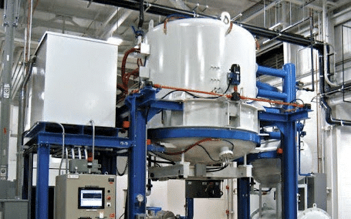
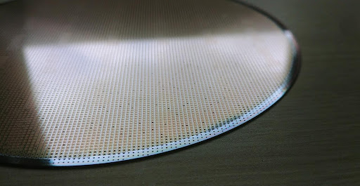
The flash furnace process is a critical step in semiconductor manufacturing, rapidly heating silicon wafers to approximately 1000°C within just one to two seconds. To prevent oxidation of previously deposited layers, wafers are processed in a nitrogen-filled chamber. Each wafer rests on a specialized quartz pedestal, featuring precise bumps and pins, and is heated using a powerful lamp located at the chamber’s apex.
Despite its efficiency, the flash furnace process faced a persistent challenge: silicon wafer breakage. Across multiple production tools, wafer breakage rates ranged between 0.001% and 0.01%. Even this seemingly small rate significantly impacted production yields, causing costly unscheduled maintenance due to fine silicon debris.
Frequent wafer breakage disrupted production schedules and necessitated repeated equipment downtime. Conventional methods, including matching parameters across tools and implementing accelerated chamber cleaning procedures, yielded limited results.
Initial attempts at troubleshooting relied heavily on parameter alignment across tools with historically lower breakage rates. Additional maintenance routines were implemented, yet the fundamental issue persisted.
Facing ongoing breakage issues, the team applied PRIZ root cause analysis, a structured, methodical approach for identifying and addressing underlying causes of manufacturing failures.
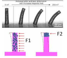
PRIZ root cause analysis revealed that wafer fractures resulted primarily from mechanical impacts caused by wafer movement during rapid heating. The flash heating process induced nitrogen pressure fluctuations, causing the wafer to shift and collide with the pedestal pins.
The PRIZ approach generated clear, actionable solutions:
Among the proposed solutions, pedestal redesign proved most effective. Engineers developed new quartz pedestal pins to securely hold wafers without causing damaging impacts. After implementing this redesigned pedestal, silicon wafer breakage was entirely eradicated from the flash furnace process.
The impact of PRIZ root cause analysis and pedestal redesign was profound, generating approximately $10 million annually in cost savings. Eliminating wafer breakage reduced production downtime, prevented wafer material loss, and significantly minimized unscheduled maintenance.
Applying PRIZ root cause analysis to the silicon wafer breakage issue demonstrated that methodical, structured troubleshooting can resolve even the most persistent manufacturing problems. This approach not only solved immediate production challenges but also positioned the semiconductor manufacturing operation for ongoing improvements in efficiency and reliability.