

The Missing Light-Absorber Mystery
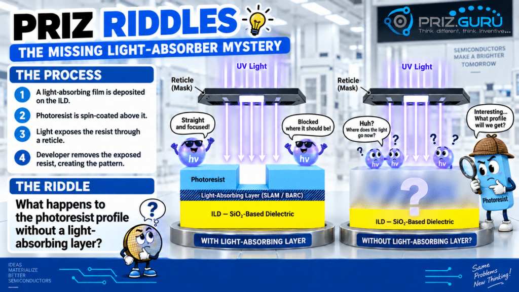
Photolithography transfers a reticle pattern into photoresist. A thin sacrificial light-absorbing layer is often placed beneath the resist even though it is removed later. Why is this temporary layer necessary?
The challenge
Creating the photoresist pattern
A typical positive-photoresist process includes four main steps:
1. Photoresist is spin-coated onto the wafer.
2. UV light exposes the resist through a reticle.
3. The exposed parts of the resist become soluble.
4. Developer removes the exposed resist and reveals the pattern required for the next etch operation.
Ideally, the developed photoresist should have straight vertical walls and the correct critical dimension.
The hidden layer
Before applying photoresist, a thin sacrificial light-absorbing material—SLAM or BARC—is deposited on the ILD. This layer does not become part of the finished device. It is removed during later processing.
Nevertheless, without it, the photoresist profile may be seriously distorted.
Your task
What happens to the photoresist profile without a light-absorbing layer?
Think first.
Before you look
What’s your answer?
Writing down a hypothesis makes the reveal more satisfying—and your reasoning easier to compare.
Your guess stays private. No account required.
I’ll skip the guessAnswer revealed
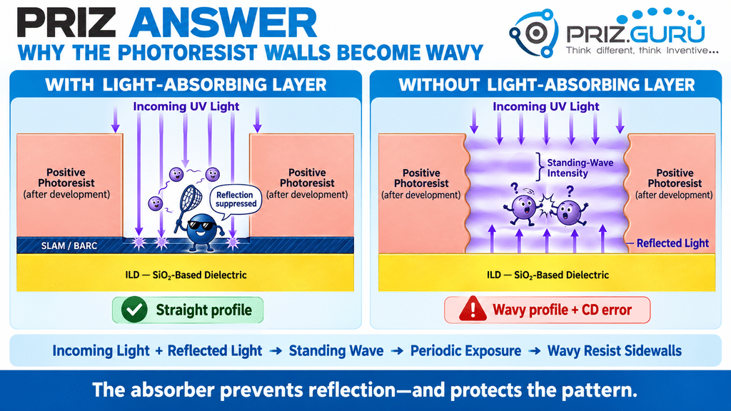
The photoresist walls become wavy.
Without the light-absorbing layer, some of the exposure light passes through the photoresist, reaches the underlying ILD, and is reflected upward.
The reflected light meets the incoming light. Their interference creates a standing wave inside the photoresist.
The standing wave produces alternating regions of high and low light intensity through the resist thickness:
Incoming light + reflected light → standing wave → periodic exposure
For positive photoresist, the strongly exposed regions dissolve faster during development, while the weakly exposed regions dissolve more slowly.
Instead of straight vertical walls, the developed resist forms wavy or corrugated sidewalls. This creates:
- critical-dimension errors,
- poor pattern fidelity,
- resist-profile variation,
- and defects that may be transferred into the ILD during etching.
Why this works
The SLAM/BARC layer absorbs the light reaching the bottom of the photoresist and suppresses reflection from the underlying material.
Without the reflected light, a strong standing wave cannot form. The exposure through the resist becomes more uniform, producing straighter sidewalls and better CD control.
No absorber → reflection → standing wave → periodic exposure → wavy resist profile
The paradox is solved: the layer is sacrificial, but its function is critical.
It removes unwanted light before that light can damage the pattern.
How did you do?
Your response helps us tune difficulty.