

The Etch-Stop Double Life
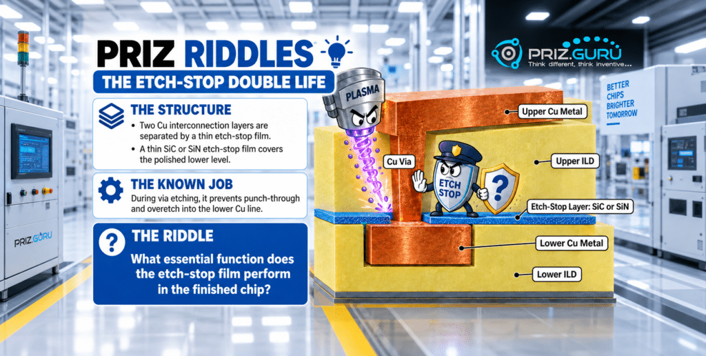
An etch-stop film protects the lower copper line during via etching, but its job does not end when fabrication is complete.
The challenge
After a Cu interconnection level is completed, its surface is polished by chemical mechanical polishing (CMP).
A thin film of silicon nitride (SiN) or a silicon-carbide-based material such as SiCN is then deposited across the polished surface. The interlayer dielectric and metal structures of the next level are built above this film.
The known job
When a via is etched through the upper dielectric, the film acts as an etch stop. It provides a controlled stopping point and prevents the plasma from punching through or overetching the lower Cu line.
But the film remains inside the finished chip and continues performing another essential function throughout the device’s operating life.
Your task
What essential function does the etch-stop film perform in the finished chip?
Before you look
What’s your answer?
Writing down a hypothesis makes the reveal more satisfying—and your reasoning easier to compare.
Your guess stays private. No account required.
I’ll skip the guessAnswer revealed
The etch-stop film is also the upper diffusion barrier and cap for copper.
Copper provides excellent electrical conductivity, but atoms and ions can migrate into the surrounding dielectric under thermal and electrical stress.
The liner around each interconnect blocks this movement through the bottom and sidewalls. After CMP, however, the top surface of the line is exposed.
The or -based etch-stop film seals this surface and completes the encapsulation:
- Ta/TaN protects the bottom and sidewalls.
- The etch-stop film protects the top.
Its dense, continuous structure creates a high-energy path for transport, strongly restricting diffusion into the upper ILD.
Without this cap, contamination can introduce electrical defects into the dielectric, increase leakage current, reduce dielectric-breakdown strength, and eventually cause device failure. The –cap interface also influences resistance to electromigration and void formation.
Why this works
The same film performs two different jobs during two stages of its life:
During fabrication: it controls the via etch and protects the lower Cu line.
During chip operation: it acts as the upper Cu diffusion barrier and helps preserve interconnect reliability.
on the bottom and sides + an or -based cap on top → remains enclosed and isolated from the dielectric.
Thinking principle: A component’s name may describe its first job—not its most important one.
Always ask what useful functions remain after the manufacturing operation is finished.
How did you do?
Your response helps us tune difficulty.