Semiconductor yield is often described as if it were a clean, objective percentage: take a wafer, count the good chips, divide by the total possible chips, and report the result.
That definition is useful as a starting point. But it is too simple to explain what really happens inside a fab.
Publicly, semiconductor manufacturers often define yield in broad terms such as the percentage of usable die produced on a wafer or the percentage of non-defective chips produced relative to the maximum possible chip count. These definitions are technically reasonable, but they leave out many of the distinctions that matter most to engineers, customers, and investors. Inside the fab, yield is tracked through a much richer set of metrics: gross yield, net yield, first-pass yield, final test yield, wafer acceptance, defect density, DPPM, bin distribution, rework loss, burn-in fallout, parametric yield, functional yield, and cost per good die.
This difference between public yield language and internal yield reality is important because yield is not just a manufacturing metric. It affects process complexity, product reliability, customer trust, financial stability, and the economics of the entire semiconductor value chain.
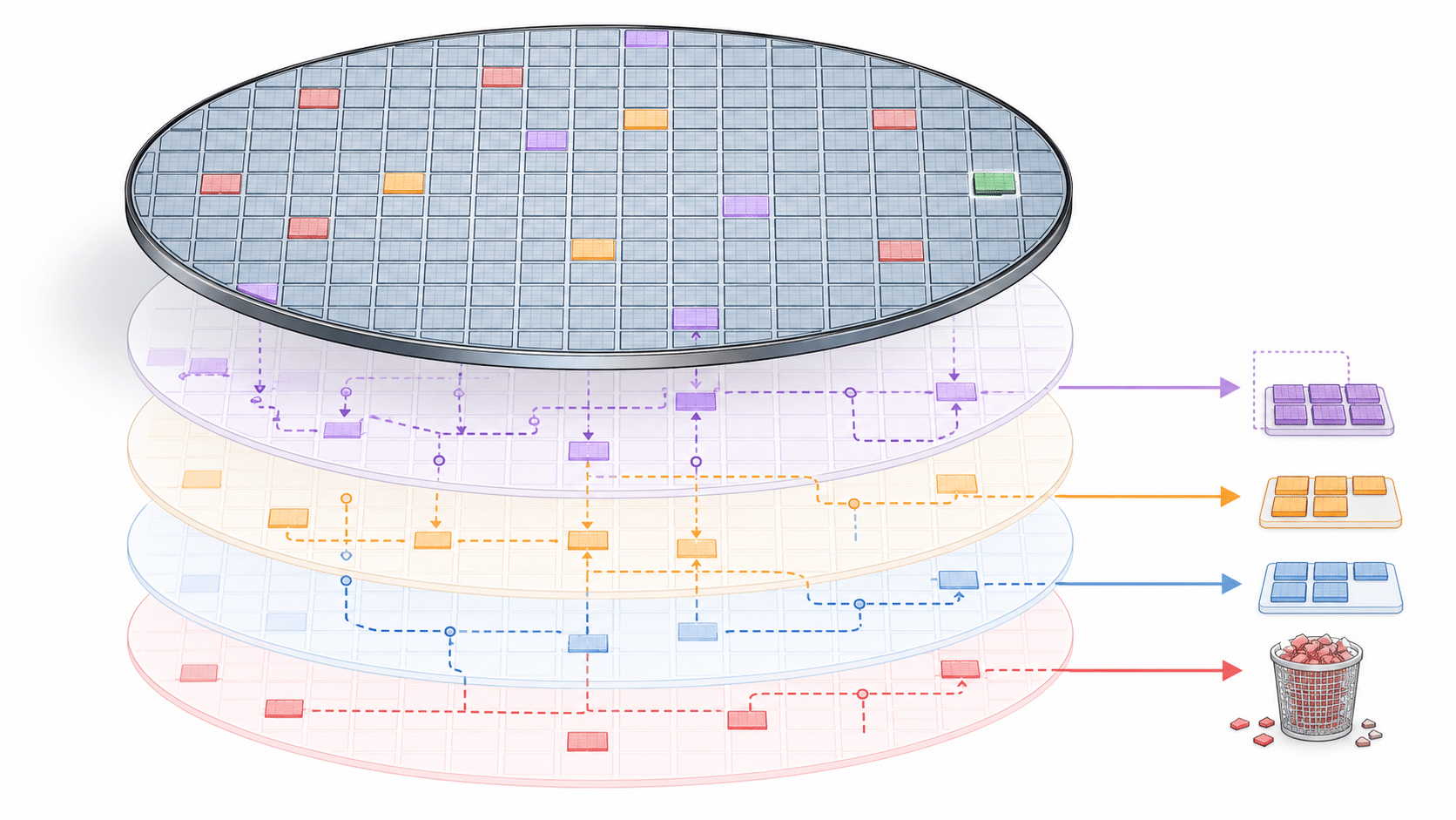
Public yield language has a clear purpose. Investors, customers, journalists, and analysts need a simple way to understand whether a process is improving, a new node is ramping, and a manufacturer can support demand.
That is why companies often discuss yield indirectly. Instead of publishing raw wafer-level yield data, they may report wafer shipments, technology mix, capacity expansion, high-volume production milestones, or general yield improvement. These signals are useful, but they are not the same as full operational transparency.
For example, a company may report strong wafer shipments and a growing share of advanced-node revenue. That information can indicate commercial success, strong demand, and manufacturing scale. It does not reveal first-pass yield, defect density, bin movement, rework cost, burn-in losses, or reliability fallout.
The public story can show that the manufacturing system is producing revenue.
Internal yield metrics show how much effort, recovery, and hidden cost were required to produce that revenue.
Inside a fab, yield is rarely treated as one final number. Engineers need to know where losses occur, how much of the output is recovered, and what those recoveries cost.
A simplified internal view may include:
These distinctions matter because final yield can improve even when process health remains weak. A die that passes cleanly on the first attempt, a die recovered through redundancy, a die that passes only after retest, and a die sold into a lower-performance bin can all contribute to final sellable output. From a revenue perspective, that recovery is definetely valuable. From a process-health perspective, each path carries a different meaning.
This is why final yield should not be interpreted in isolation. It tells us what eventually became sellable. It does not necessarily tell us how stable, efficient, or reliable the manufacturing process was along the way.
Binning is one of the reasons public yield can appear stronger than the raw process story would suggest.
In many semiconductor products, chips are tested and sorted by performance. A chip that fails to meet the highest speed, voltage, or power target may still meet the requirements for a lower-tier product. Selling that chip into a lower bin is legitimate and economically useful. It reduces waste and allows more of the wafer to become revenue-generating product.
The question is what the bin distribution says about process health.
When more chips slide from premium bins into lower bins, shipment volume can still look healthy while the economics underneath weaken. The process window may be getting tighter, variation may be taking more space, and defect mechanisms may be pushing value out of premium categories into lower-margin products. The company may still be shipping product, but the mix is telling a more complicated story than the top-line yield number suggests.
The same principle applies to redundancy, especially in memory. Spare rows, columns, or blocks can rescue die that would otherwise fail. This means that “usable” does not always mean “clean.” A rescued die and a clean first-pass die both contribute to output, yet they say very different things about the process.
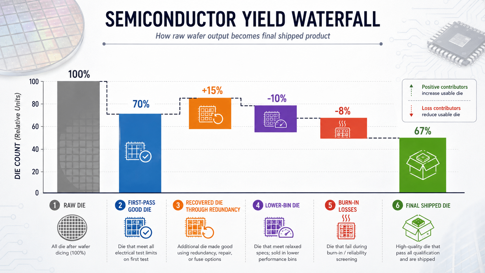
First-pass yield is one of the most important indicators of process discipline because it shows how much good output the system produces without extra recovery.
Final yield tells us what eventually shipped.
First-pass yield tells us how naturally the process produced good output before rework, retest, additional screening, or other corrective loops.
This distinction has major operational consequences. A fab with strong first-pass yield is usually easier to scale, easier to schedule, and easier to stabilize. A fab with weak first-pass yield may still reach acceptable final output, but only by consuming additional resources.
The hidden cost is often a “factory inside the factory”: repeated inspections, engineering holds, manual reviews, rework loops, retesting, disposition meetings, and urgent containment activity. These actions do not appear clearly in a public yield percentage, instead, they show up later as cost, delay, capacity loss, and organizational fatigue.
For mature processes, weak first-pass yield points to unmanaged variation, poor process discipline, or unresolved equipment interactions. For advanced nodes, it reflects a narrow process window, incomplete mechanism understanding, or design-manufacturing interactions that require deeper investigation.
A final yield number can answer whether product shipped.
First-pass yield helps answer whether the process is actually healthy.
Every semiconductor process is already a complex chain of dependencies. Lithography, etch, deposition, cleaning, CMP, metrology, electrical test, packaging, and final qualification all interact. A local improvement in one area can create a downstream issue somewhere else.
Yield problems add another layer of complexity. When losses appear, teams often respond with more inspection, tighter controls, additional test steps, engineering reviews, temporary containment actions, and new disposition rules. Many of these actions look as justified in the moment. Over time, they often become a permanent additions to the process.
The result is a heavier manufacturing system. Cycle time increases, decision-making slows, and engineers spend more time managing exceptions. Instead of becoming simpler and more robust, the process becomes better at catching failures after they occur.
This is one of the most important lessons in sustainable yield improvement. Improving yield by adding more filters is different from improving yield by removing the cause of variation. A healthy process should become easier to control over time, not more dependent on corrective operations.
Yield and reliability are connected, yet they are not the same.
Yield tells us whether a die passed a defined set of tests at a defined point in the manufacturing flow.
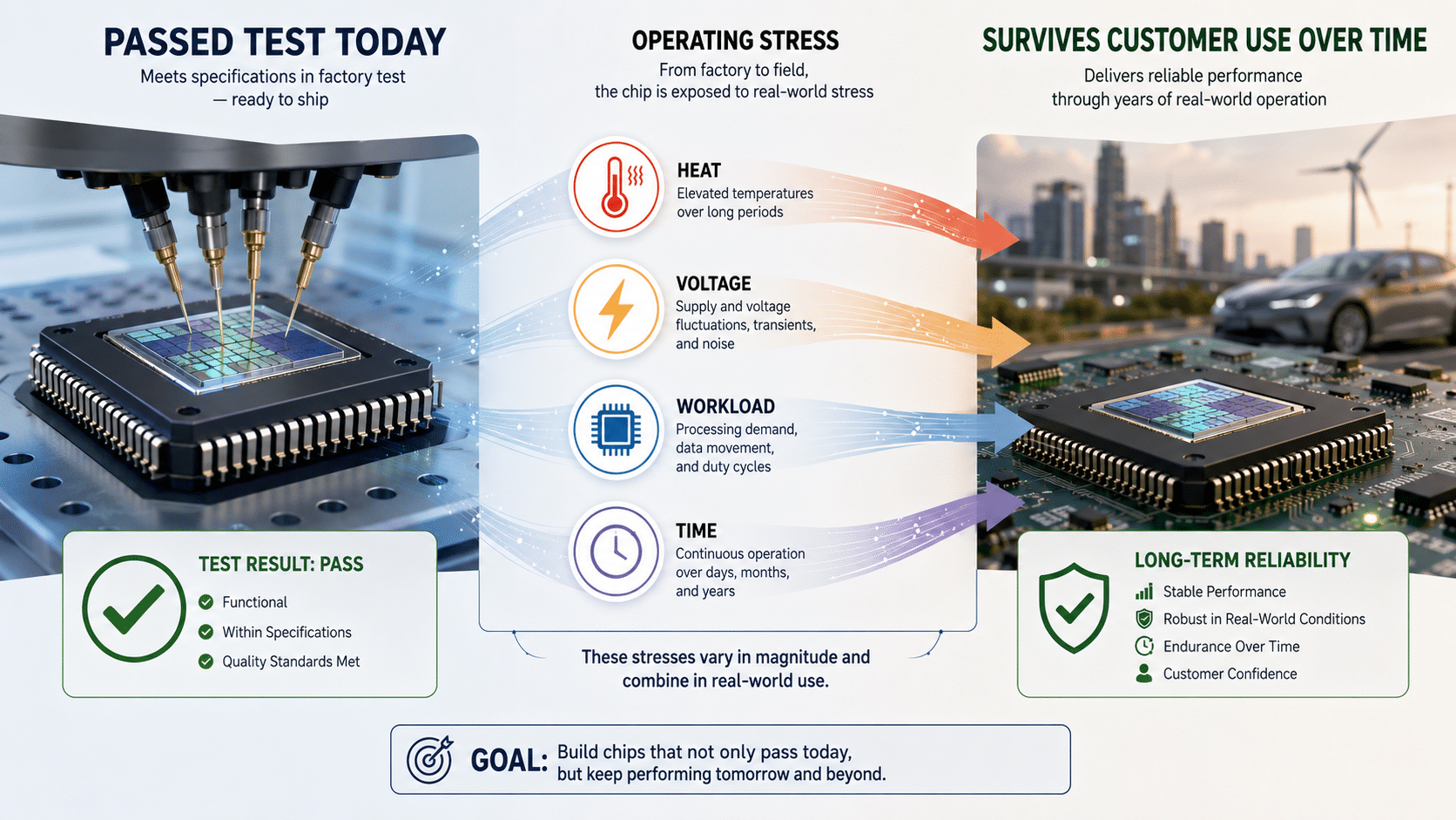
Reliability asks whether the product will continue to perform under temperature, voltage, workload, aging, and customer use.
A chip can pass production test and still carry marginal behavior. That behavior may appear later as early-life failure, intermittent instability, degraded performance, field returns, or customer qualification problems.
This is why DPPM, burn-in fallout, guardband behavior, and bin distribution matter so much. These metrics help reveal the health of the population that leaves the factory.
For consumer products, marginal reliability can cause inconvenience and brand damage. For automotive, aerospace, medical, industrial, and data-center applications, reliability weakness can become a much larger business and safety concern.
Final yield says the product passed.
Reliability asks how much confidence we should have in that pass.
For companies that own fabs, such as Intel, Samsung, and TSMC, yield directly affects the economics of production.
A fab carries enormous fixed cost. Equipment, cleanrooms, depreciation, energy, chemicals, maintenance, metrology, and engineering support remain expensive whether the wafer produces many good dies or many bad dies.
When yield drops, cost per good die rises.
That is the simplest financial truth in semiconductor manufacturing.
A wafer with poor yield consumes the same expensive capacity as a wafer with strong yield. It uses the same tool time, cleanroom space, materials, and engineering infrastructure. The difference is how many sellable chips emerge at the end.
For a high-demand product, poor yield also creates opportunity cost. Every bad die represents lost revenue from scarce capacity. In AI, advanced logic, high-bandwidth memory, and advanced packaging, that lost capacity can be extremely valuable.
Yield therefore hits fabs in multiple places at once:
This is why a single yield point can matter. In a large fab or advanced-node operation, a small percentage change can represent millions, tens of millions, or even hundreds of millions of dollars depending on wafer volume, die size, wafer cost, selling price, and demand.
Yield is not a factory detail. It is a financial control knob.
Fabless companies do not own the manufacturing process in the same way. A company like Lattice Semiconductor relies on external foundries and manufacturing partners rather than operating leading-edge fabs itself. That changes the exposure, but it does not eliminate it.
For fabless companies, yield problems show up through pricing, supply availability, delivery commitments, product qualification, gross margin, and customer trust. The foundry owns many of the process levers. The fabless company owns the product promise. That is a difficult position.
If yield is weak at the foundry, the fabless company may face limited supply, higher costs, delayed ramps, or difficult allocation decisions. The company may also have less visibility into the root cause than an integrated device manufacturer would have. So the business risk moves downstream.
The defect mechanism may live in the fab. The customer escalation may land on the fabless supplier.
This distinction is important when comparing companies like Intel, Samsung, and TSMC with companies like Lattice. The former carry direct manufacturing economics. The latter carry supply-chain and margin exposure. Both are affected by yield, but the pain arrives through different paths.
Customers usually do not ask suppliers for detailed yield curves. They care about product availability, price, quality, performance, and delivery confidence. Yield affects all of those.
When yield is weak, supply becomes tighter, prices rise, premium bins become harder to obtain. Lead times stretch and product launches may slip. Customers often pushed toward alternative parts, lower performance options, or redesigns.
In some markets, this is manageable, others not som much.
In automotive, aerospace, medical, industrial, and infrastructure applications, changes are slower and more expensive. A qualified semiconductor is not easily replaced. A supply issue can ripple into boards, systems, certifications, factory schedules, and end-customer commitments.
The customer does not need to see the yield report to absorb its consequences. Those consequences show up as higher prices, longer lead times, larger inventory buffers, reduced design flexibility, and, over time, the decision to qualify a second supplier.
That last cost is easy to underestimate. Once trust is damaged, customers rarely say, “We are leaving because your yield story was too optimistic.” They simply redesign the next platform differently.
Semiconductor economics are often discussed through demand, capacity, capital expenditure, and technology leadership. Yield sits underneath all of these topics.
A company can have strong demand and still struggle economically if yield is weak. A new process node can be technically impressive but financially difficult if cost per good die remains too high. A product can be architecturally strong but commercially constrained by die size, defect density, package yield, or bin distribution.
Advanced technologies raise the stakes because process windows are tighter, equipment costs are higher, die can be larger, and customer expectations are unforgiving. In this environment, yield performance influences not only manufacturing cost but also pricing, availability, market timing, and competitive position.
This creates a paradox. Yield is one of the most important economic variables in semiconductors, yet it is one of the least transparent public metrics. There are good reasons for that. Detailed yield data is competitively sensitive and can reveal process weakness, customer exposure, cost structure, and ramp maturity. Still, limited transparency makes it harder for all stakeholders to understand the true health of a semiconductor business. A company may look strong through revenue and shipments while certain products, nodes, or customer programs carry significant hidden yield cost.
The goal is not to expect semiconductor companies to publish every internal yield curve, wafer map, defect count, or customer-specific process metric. That would be unrealistic and commercially risky.
The better goal is to ask more precise questions.
Instead of asking only, “What is the yield?” one should ask:
These questions move yield from a public comfort metric to an operational truth system. They also help distinguish between temporary recovery and real process learning.
A public yield statement can be technically accurate, legally acceptable, and still incomplete as a picture of manufacturing health.
A final yield number may include the benefits of rework, binning, redundancy, burn-in, sampling, product mix, and reporting boundaries. Each adjustment can be reasonable. Taken together, they create a more optimistic view than raw internal metrics would suggest.
This does not mean the public number is false. It means the number needs context.
A serious yield discussion should ask what failed, where it failed, how it was recovered, and whether the underlying mechanism was removed. It should distinguish between yield improvement caused by better process control and yield improvement caused by better recovery, filtering, or reporting boundaries.
That distinction matters because a process can look better before it actually becomes better.
Sustainable yield improvement does not come from chasing a percentage. It comes from understanding the mechanisms behind loss.
A fab improves yield when teams understand why defects occur, how variation propagates, which process functions are unstable, where interactions are hidden, and which corrective actions reduce complexity rather than adding more control layers.
Extra inspection can catch more failures. Rework can recover some value. Binning can protect revenue. Burn-in can screen weak devices. But none of them replace mechanism-level understanding.
The strongest semiconductor teams build a continuous learning cycle around yield. They define the problem precisely, map the process, identify failure mechanisms, test assumptions, remove causes, capture learning, and reuse that learning across future problems.
That is how yield improvement becomes more than firefighting. It has to become organizational knowledge.
Semiconductor yield is often presented publicly as a simple percentage. Inside the fab, it is a much richer signal of process health, product risk, engineering discipline, and economic performance.
The public number matters because it helps the market understand progress. The internal truth matters because it determines cost, reliability, capacity, customer trust, and long-term competitiveness.
Companies that treat yield mainly as a reporting metric will keep improving the story around the process. Companies that treat yield as a mechanism problem have a better chance of improving the process itself.