Copper electroplating is essential for forming advanced semiconductor interconnects, yet radial thickness non-uniformity remains a costly challenge. Thicker deposition at the wafer edge and thinner copper at the center force manufacturers to rely on overplating and CMP compensation, increasing material waste and process cost.
In this article, we use the PRIZ Platform to show that the true amplification mechanism lies in operating within a kinetically controlled environment, where small voltage variations caused by seed-layer resistance produce large thickness deviations. By shifting the process closer to diffusion-controlled behavior and reducing sensitivity to voltage fluctuations, uniform deposition can be achieved intrinsically — enabling thinner seed layers, reduced overplating, lower CMP burden, and overall cost reduction.

Copper electroplating is a foundational process in modern semiconductor manufacturing, a key step in the damascene process. In advanced BEOL (Back-End-of-Line) integration, copper electrodeposition is used to fill high-aspect-ratio vias and trenches that form the interconnect network of microchips.
The method is widely adopted because it is:
A wafer coated with a thin copper seed layer is immersed in an electrolyte containing copper sulfate and sulfuric acid, along with carefully engineered additives. When DC voltage is applied, copper dissolves at the anode and deposits on the wafer surface.
In theory, if the applied potential is uniform, the deposited thickness should also be uniform.
In practice, it is not.
In real production environments, copper thickness is:
This radial non-uniformity is a well-known issue in electroplating.
The wafer is electrically contacted at the bevel. The copper seed layer, intentionally kept thin for cost and integration reasons, has finite sheet resistance. The electricity is connected through the contact on the wafer bevel. Current must travel laterally through this resistive film.
As the distance from the electrical contact increases:
The result is thicker copper near the edge and thinner copper in the center. The process behaves exactly according to physics, but not according to manufacturing goals.
Rather than eliminating the root cause, industry typically compensates for it.
More copper is deposited than required. The excess is removed by Chemical Mechanical Polishing (CMP).
This results in deposition and removal of additional copper that is not functionally necessary. Such a solution increases:
We deposit material we do not need, and then we remove it.
A conductive ring near the wafer edge diverts part of the current to reduce peripheral deposition.
Uniformity improves, but copper is deposited on a non-functional surface. Again, energy and material are consumed without adding product value.
These approaches protect yield. They do not eliminate the inefficiency.
Neither method solves the problem, but they just try to compensate for the failure, a symptom.

Using the PRIZ Platform, the problem was analyzed with:
The analysis revealed a deeper insight.
The system is not only affected by seed resistance. The non-uniformity is amplified because the electroplating process operates primarily in the kinetically controlled regime of the polarization curve. The process is performed in conditions where the electrical current strongly depends on the applied voltage.
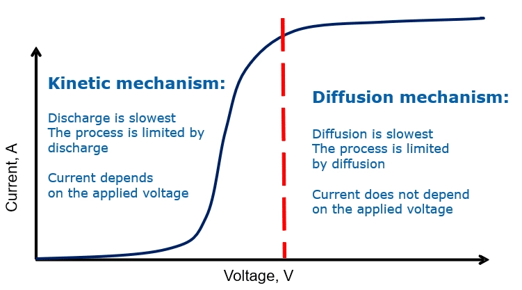
Electrodeposition follows a current–voltage (polarization) relationship.
There are two fundamental regimes:
This means:
Small IR drop → large change in current → large thickness variation.
In this regime:
Small voltage variations → minimal change in current → stable thickness.
PRIZ analysis revealed that the electroplating process is operating in a regime that is highly sensitive to local voltage variations. The seed resistance creates small potential differences, but because the process is kinetically dominated, those small differences are amplified into large thickness deviations.
This is the true mechanism behind the problem.
The objective is not:
The objective is:
Reduce the sensitivity of deposition rate to local voltage variations.
This means shifting the operating point of the process closer to the diffusion-controlled regime.
When deposition becomes diffusion-limited:
Instead of compensating for physics, we redesign the system so physics works in our favor.
PRIZ analysis generated several strategic solution paths aimed at reducing the sensitivity of copper deposition to local voltage variations and shifting the process closer to diffusion-controlled behavior.
Adjust the operating voltage to move the process closer to the diffusion-limited region of the polarization curve, where current becomes less sensitive to small voltage variations.
In practice, this is not trivial when operating under a galvanostatic regime (constant current), since the system automatically adjusts voltage to maintain current. Achieving a controlled shift in operating conditions may require reconsidering the power supply strategy, potentially transitioning toward a potentiostatic or hybrid control regime.
This is not a simple parameter change — it requires careful electrochemical engineering to ensure:
This is exactly where structured engineering thinking becomes essential.
A moderate increase in electrolyte temperature (for example, 5–10 °C) can alter the balance between charge-transfer kinetics and mass transport.
Temperature increases:
Because reaction kinetics are typically more temperature-sensitive than diffusion, raising temperature can help reduce kinetic limitation and shift the operating point toward a more stable regime.
However, thermal effects on additive stability and bath lifetime must also be considered.
Pulsed or modulated current deposition introduces controlled dynamic behavior into the system.
Short high-current pulses can enhance discharge kinetics, while off-times allow concentration gradients to relax and diffusion to re-establish equilibrium.
Properly engineered pulse parameters (frequency, duty cycle, peak current) can:
This approach enables control over the effective electrochemical regime without permanently increasing average current density.
Instead of compensating with a dummy cathode that consumes material, the electric field itself can be engineered.
A key question arises:
Why must the anode diameter match the wafer diameter?
A smaller or reshaped anode may alter field distribution and current line geometry, potentially reducing peripheral current concentration and improving central deposition.
Unlike a dummy cathode, this approach does not waste copper on non-productive surfaces. It modifies the system geometry to influence current distribution directly.
This direction requires modeling of electric field and current density distribution to validate effectiveness.
Each of these approaches aims to reduce kinetic dominance, stabilize current density across the wafer, and achieve intrinsic deposition uniformity without increasing seed thickness or relying on wasteful compensation.
Visit the PRIZ Hub to explore the full project analysis and solution pathways.
If uniformity is achieved intrinsically rather than through compensation:
This is not incremental optimization. It is a system-level redesign based on understanding functional contradictions.
Copper electroplating does not fail because of resistance alone. It fails because the process amplifies small voltage variations in a kinetically sensitive regime.
By shifting the electrochemical operating point toward diffusion control, we reduce that amplification.